
The semiconductor industry has long relied on Moore’s Law as its guiding principle, but the slowing of transistor scaling has forced engineers to seek new paradigms. Instead of shrinking devices further on a single die, innovation is now centered on stacking, interconnecting, and packaging. Erik Hosler, a veteran in lithography and advanced integration strategies, recognizes that the progression from 2.5D to 3D packaging represents not just an engineering milestone but a new framework for sustaining performance in the post-Moore era.
This shift marks a redefinition of progress. No longer measured solely by transistor density, advancement is increasingly gauged by how effectively multiple chips can be combined into a single, high-performing system. Packaging has become the new frontier where electrical, thermal, and mechanical design converge. The roadmap that stretches from 2.5D Integration to 3D stacking and beyond reflects a broader recalibration of Moore’s Law itself. For the industry, this development signals not the end of innovation, but the beginning of a different kind of scaling.
The 2.5D Foundation
The move toward advanced packaging began with 2.5D Integration, where dies are placed side by side on an interposer that manages connections. This approach provided significant improvements in bandwidth and power efficiency compared with traditional system-on-chip designs, without the yield risks of stacking. It marked a pivotal shift, showing that innovation in placement and interconnect could rival raw transistor scaling in driving progress.
2.5D Integration proved especially valuable for high-performance computing and graphics, where wide memory bandwidth was crucial. By decoupling memory and logic dies while maintaining fast interconnects, 2.5D enabled systems that would have been impossible on a single monolithic die. It demonstrated that packaging could be a performance enabler in its own right, laying the groundwork for more ambitious vertical Integration. This success gave the industry confidence that packaging would develop into a core design strategy rather than remain a supporting function.
The Leap to 3D Integration
Building on this foundation, 3D Integration represented a true leap. By vertically stacking dies connected through through-silicon vias, engineers could bring logic and memory into close physical proximity, reducing latency and boosting performance per watt. This density opened opportunities for AI, data centers, and mobile devices alike.
Yet with these gains came new challenges. Heat management, yield sensitivity, and bonding precision became limiting factors. Advanced cooling, inspection, and metrology tools were required to make 3D Integration practical at scale. The cost of yield loss in stacked devices is particularly high: if one die fails, the entire stack can be compromised, increasing the pressure on fabs to refine bonding processes and defect detection. Thermal bottlenecks also intensify in stacked systems, demanding novel approaches to materials, packaging design, and cooling strategies. These realities underscored that 3D Integration was not just a technical step forward but a transformation in manufacturing economics and reliability.
Beyond 3D: Hybrid and Heterogeneous Futures
As 3D matures, the roadmap points toward hybrid Integration that combines multiple technologies in a single package. Logic, memory, photonics, and even quantum components may one day coexist within tightly integrated systems. These heterogeneous packages could redefine the boundaries of computing by balancing speed, efficiency, and specialization. In effect, Integration itself becomes the new engine of progress, allowing diverse technologies to work in harmony.
The industry is also exploring chiplets, modular dies that can be assembled in flexible combinations. This approach promises cost savings, better yields, and customizable system designs. Together, hybrid 3D and chiplet-based approaches extend the spirit of Moore’s Law into an era defined not by transistor count, but by system-level innovation. Packaging thus becomes the lens through which the future of computing will be determined. By shifting focus from shrinking devices to orchestrating systems, the industry secures a more adaptable and resilient path forward.
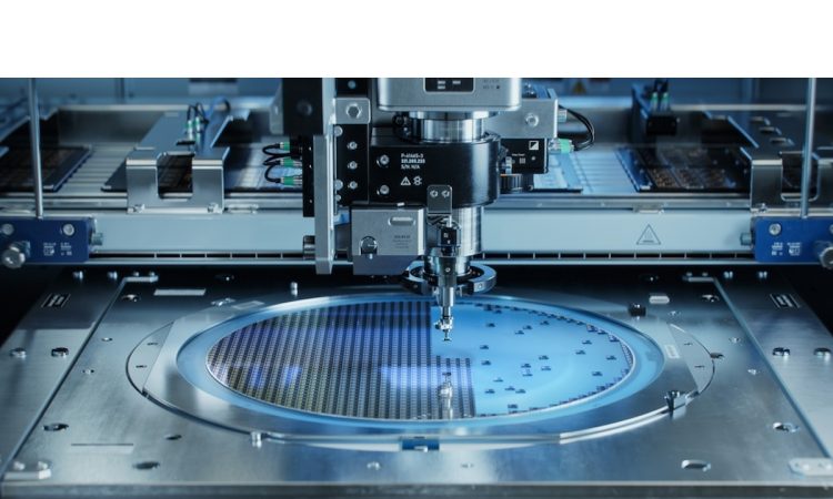
Precision Tools Guiding the Roadmap
The path from 2.5D to 3D and beyond requires more than bold concepts, but it depends on tools that can achieve atomic-scale accuracy. Aligning dies, bonding layers, and detecting defects demand inspection and metrology systems capable of unprecedented precision. These tools are the invisible backbone of the post-Moore roadmap. Without them, even the most visionary designs would remain theoretical rather than manufacturable.
Erik Hosler explains, “Tools like high-harmonic generation and free-electron lasers will be at the forefront of ensuring that we can meet these challenges.” His insight illustrates that the future of packaging is inseparable from the development of manufacturing. Without precise control, even the most promising architectures cannot scale. It is precision that transforms ambitious roadmaps into reliable technologies.
Implications for Moore’s Law Alternatives
This packaging roadmap reframes the industry’s relationship with Moore’s Law. Instead of relying on smaller transistors, progress now comes from integration density, interconnect efficiency, and system heterogeneity. Performance scaling continues, but along a different axis.
The implications are profound. Design strategies, investment priorities, and workforce skills must adapt to a world where packaging is central. Leading fabs are already reallocating capital toward bonding and inspection tools, while design houses are training engineers in packaging-aware architectures. Governments are funding packaging research as part of national competitiveness strategies, underscoring that this development is as much geopolitical as it is technological. In short, packaging is no longer a supporting act but the stage itself, where the future of computing performance will play out.
Charting the Path Beyond Moore’s Law
The journey from 2.5D to 3D and beyond shows that semiconductor innovation is far from reaching its limits. By reimagining packaging as the driver of progress, the industry has opened doors to architectures that balance performance, power, and cost in entirely new ways. The roadmap demonstrates that scaling is not dead, but it has simply shifted into new dimensions. This development confirms that the essence of Moore’s Law endures, even if its form has changed.
The next era will be shaped by how effectively heterogeneous Integration, chiplets, and emerging technologies like photonics are packaged together. With precision tools guiding the process, packaging is positioned to become the defining force in post-Moore computing. Those who lead in this transition will not only extend Moore’s legacy but also shape the next paradigm of digital progress. In doing so, they will determine the pace and direction of global innovation for decades to come.

